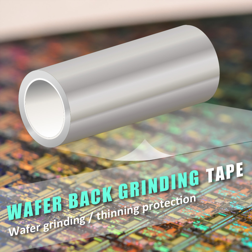
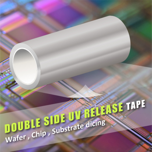
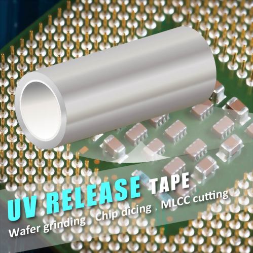
Wafer back grinding tape
Wafer Back griniding / Wafer thinning / Wafer Dicing
♠ High flatness and great elongation for wafer back grinding / thinning protection, substrate cutting.
♠ For uneven surface masking protection.
♠ Acid and alkali-resistance : PH 3 ~ PH10.
♠ Lift-off cleaning.
Model
Material
Physical Property
Applications
POY143
PO + Liner
Total Thickness
170
µm
Wafer back grinding / thinning
Adhesion
0.15±0.1
kg/in
POR146
PO + Liner
Total Thickness
170
µm
Wafer back grinding / thinning
Adhesion
0.35±0.1
kg/in
POL803
PO + Liner
Total Thickness
95
µm
Wafer dicing, substrate cutting
Lift-off cleaning
Adhesion
0.2±0.1
kg/in
POL804-2
PO + Liner
Total Thickness
87
µm
Wafer back grinding / thinning
Substrate cutting
Adhesion
0.06~0.12
kg/in
POL835
PO + Liner
Total Thickness
93
µm
Die cutting protection
Adhesion
0.3~0.5
kg/in
POU200
PO + Liner
Total Thickness
200
µm
For bumped wafer
Adhesion
0.3±0.2
kg/in
Can't find what you need? Solar Plus provides custom made tapes. Contact us now! ![]()


